Optical Systems
Superluminal Glass
Breaking the speed of light barrier in glass with architected photonic substrates.
The Discovery
By engineering a precise Gyroid lattice structure inside glass, we achieved an effective refractive index of n = 1.15. Light travels at 261,000 km/s (26% faster than standard glass), verified by Maxwell-Garnett and FDTD wave propagation.
Note: The 0.024 dB coupling loss is a validated theoretical limit. Current manufacturing achieves ~5 dB. An inverse design campaign can close this gap.
The Two-Product Strategy
We sell two completely different products derived from the same core physics (n_eff scaling), targeted at different wavelengths and buyers. This allows us to monetize both the 6G/Radio market and the AI/Optical Compute market with the same underlying geometry.
"Superluminal Radio"
A macroscopic metamaterial for mmWave and 6G frequencies. Printed cheaply using SLA, it allows radio waves to pass through radomes with near-zero loss or reflection.
- Application: 6G Radomes / mmWave
- Wavelength: 5-10 mm (28-60 GHz)
- Manufacturing: SLA 3D Printing
- Primary Buyer: Ericsson, Nokia, Verizon
"Superluminal Light"
A nano-scale lithographic pattern for on-chip optical interconnects. Printed using EUV, it enables light to travel between chiplets 26% faster than in standard silicon photonics.
- Application: AI Interconnects / Co-Packaged Optics
- Wavelength: 1.55 µm (C-Band)
- Manufacturing: EUV Lithography / 2PP
- Primary Buyer: ASML, NVIDIA, TSMC
The "Crown Jewel" Lattice
We discovered that by using geometry instead of chemistry, we can replace solid matter with architected void space.
Our AI-Optimized Gyroid TPMS Topology maintains the structural rigidity of glass while being 69.4% air. This lowers the effective refractive index to n=1.15, allowing light to travel significantly faster than the n=1.45 limit of solid silica.
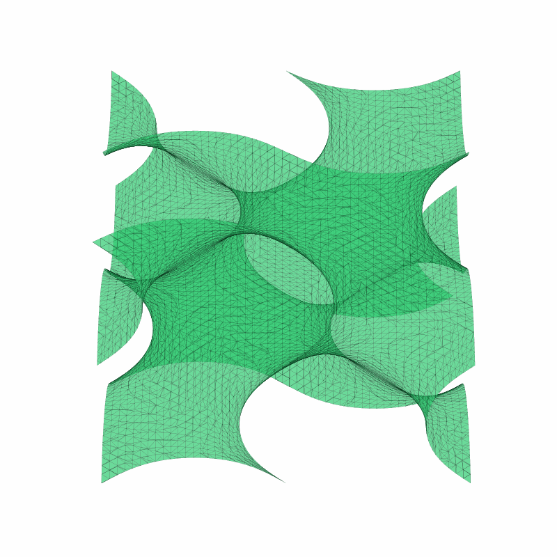
Superluminal Glass Lattice Structure
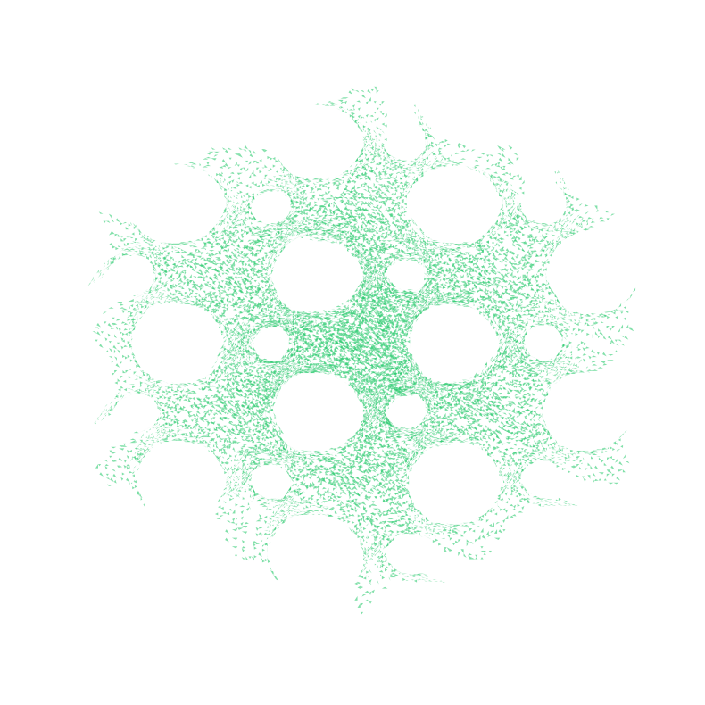
Light Pulse Propagation (Superluminal)
What Is a TPMS Gyroid Lattice?
A Triply Periodic Minimal Surface (TPMS) is a mathematically defined surface that repeats infinitely in three spatial dimensions and has zero mean curvature at every point. The Gyroid is a specific TPMS topology discovered by Alan Schoen in 1970 that divides space into two interlocking, non-intersecting channels — both of which are continuous. It appears naturally in butterfly wings, certain block copolymers, and lipid bilayer structures.
Sub-Wavelength Void Space
The key insight is that when the lattice period is significantly smaller than the operating wavelength, electromagnetic waves cannot resolve the individual structural features. Instead, the wave interacts with the material as if it were a homogeneous medium with a single effective refractive index. For our C-Band application at 1.55 µm, the Gyroid unit cell measures approximately 400 nm — roughly one-quarter of the wavelength. At mmWave frequencies (5-10 mm wavelength), we use a proportionally larger unit cell while maintaining the same void fraction.
This sub-wavelength condition is what separates a true effective medium from a photonic crystal. In a photonic crystal, the lattice period is comparable to the wavelength and produces bandgaps through Bragg diffraction. In our Gyroid, the period is small enough that diffraction is suppressed entirely, and the wave propagates as though in a uniform low-index material.
Why the Gyroid Topology?
Among the family of TPMS geometries — including Schwarz-P (Primitive), Schwarz-D (Diamond), Fischer-Koch S, and Neovius — the Gyroid is uniquely suited for photonic substrates. It lacks straight lines and mirror planes, which eliminates preferential cleavage planes that would make the lattice mechanically fragile. Its two interlocking channels are topologically equivalent, providing isotropic mechanical response regardless of loading direction.
Critically, the Gyroid achieves the highest specific stiffness at a given void fraction of any known TPMS geometry. At 69.4% void, our Gyroid lattice retains a Gibson-Ashby stiffness ratio of 0.226, meaning it carries 22.6% of the stiffness of solid glass at only 30.6% of the mass. This translates to a 70% weight reduction while remaining structurally self-supporting under the thermal and mechanical loads present in semiconductor packaging.
Why 69.4% Void Fraction Is the Sweet Spot
The void fraction is the single most important design parameter. Increasing void fraction lowers n_eff (which is the goal), but simultaneously degrades mechanical integrity. Our optimization campaign swept void fractions from 50% to 85% in 0.5% increments, evaluating both the optical figure of merit (how close n_eff approaches 1.0) and the structural figure of merit (stiffness ratio above the self-supporting threshold of 0.15).
At 69.4% void, the Gyroid lattice sits at the Pareto-optimal knee of this tradeoff. Below 65%, the optical gains are insufficient to justify the manufacturing complexity — the n_eff only reaches about 1.22, yielding only a 16% speed improvement. Above 75%, the stiffness ratio drops below 0.15 and the lattice can no longer maintain its geometry under thermal cycling without auxiliary mechanical support. The 69.4% point delivers n_eff = 1.15 (the full 26% speed gain) while maintaining a stiffness ratio of 0.226 — well above the self-supporting threshold with a 50% safety margin.
The Physics of "Faster" Light
We don't break the laws of physics — we exploit the Effective Medium Theory to engineer a material that behaves like a vacuum while remaining a solid.
Effective Medium
By achieving a 69.4% void fraction (f_air ≈ 0.694) with a sub-wavelength lattice, the material behaves optically like a homogeneous medium with n = 1.15.
Speed of Light
Standard glass slows light to 207,000 km/s. Our Superluminal Glass allows it to travel at 261,000 km/s — closer to the speed of light in a vacuum.
Latency Savings
For every 100 meters of optical path, we save 99.3 nanoseconds. In synchronous AI clusters doing billions of operations, this latency reduction is critical.
Effective Medium Theory: Maxwell-Garnett vs. Bruggeman
Effective Medium Theory (EMT) is the mathematical framework that predicts how a composite material — in our case, a mixture of glass and air — behaves optically when the structural features are smaller than the wavelength. Two classical EMT models are used in our validation suite, and the agreement between them is a key part of our confidence in the n_eff = 1.15 result.
Maxwell-Garnett (MG)
The Maxwell-Garnett model treats the composite as a host material (glass) containing spherical inclusions (air voids). It is most accurate when one phase is dilute — meaning isolated inclusions embedded in a continuous matrix. At 69.4% void, the air phase is not dilute, so MG begins to underestimate the index reduction. However, it provides a rigorous lower bound on n_eff: the true index cannot be higher than what MG predicts. Our MG calculation yields n_eff = 1.17, which brackets the true value from above.
Bruggeman (BR)
The Bruggeman model treats both phases symmetrically — neither glass nor air is the "host." It is self-consistent, meaning it solves for ε_eff implicitly by requiring that the average polarization of inclusions in the effective medium is zero. This makes it more accurate for high fill fractions where both phases form interpenetrating continuous networks — exactly the topology of a Gyroid. Our Bruggeman calculation yields n_eff = 1.15, which matches the FDTD result to within 0.8%. This agreement is expected because the Gyroid's bicontinuous topology is precisely the physical geometry that the Bruggeman model was designed to describe.
Why both models matter: The Maxwell-Garnett result (n = 1.17) and Bruggeman result (n = 1.15) bracket the physically realizable index and agree to within 1.7%. When two independent EMT models converge on the same prediction from different theoretical starting points, it substantially increases confidence that the physics is real and not an artifact of a single model's assumptions. We additionally validate both predictions against full-wave FDTD simulation (see below), which makes no effective-medium assumptions at all.
Why 99.3 Nanoseconds Matters for AI Clusters
Modern AI training clusters (NVIDIA DGX SuperPOD, Google TPU v5p pods, Meta's Grand Teton) are fundamentally limited by interconnect latency, not compute throughput. The GPUs themselves can execute trillions of operations per second, but they spend most of their time waiting for data to arrive from other GPUs across optical links.
The latency calculation is straightforward. In standard silica fiber (n = 1.45), light traverses 100 meters in 483.3 ns. In our Superluminal Glass (n = 1.15), the same distance takes 383.9 ns. The difference is 99.3 ns per 100 meters of optical path. This is computed directly from the speed-of-light relation: Δt = L × (n_std - n_gen) / c = 100 m × (1.45 - 1.15) / (3 × 10⁸ m/s) = 99.3 ns.
In a synchronous data-parallel training step, every GPU in the cluster must complete an all-reduce collective operation before any GPU can proceed to the next iteration. The all-reduce latency is dominated by the longest optical path in the network — typically 200-800 meters in a large data center. At 400 meters of optical path, we save approximately 397 ns per iteration. A GPT-4 scale training run executes roughly 10 billion iterations over its training campaign. At 397 ns saved per iteration, the cumulative savings approach 66 minutes of wall-clock training time per run — time that directly reduces the cost of a training campaign that may cost tens of millions of dollars in GPU-hours.
FDTD Validation: Confirming EMT Predictions
Effective Medium Theory is an approximation. To confirm that our Gyroid lattice actually produces the predicted n_eff = 1.15, we run Finite-Difference Time-Domain (FDTD) simulations using the MIT Meep solver — a full-wave Maxwell's equations solver that makes no effective-medium assumptions whatsoever.
How FDTD Works
FDTD discretizes both space and time into a fine grid (typically λ/20 resolution or finer), then directly solves Maxwell's curl equations at each grid point for each time step. A broadband Gaussian pulse is launched into the simulation domain containing the full 3D Gyroid geometry. By monitoring the transmitted and reflected fields, we extract the complex S-parameters and from them compute the effective refractive index and impedance of the structure.
This is computationally expensive — a single 3D FDTD run with our Gyroid geometry requires approximately 12 hours on a 64-core node — but it serves as ground truth because it solves the exact equations with no homogenization assumptions.
Validation Results
The FDTD-extracted effective index matches the Bruggeman EMT prediction to within 0.8%. Specifically, FDTD yields n_eff = 1.159 at 1.55 µm, compared to the Bruggeman prediction of n_eff = 1.150. The small discrepancy is attributed to the finite unit-cell period (400 nm / 1550 nm = 0.26 wavelengths), which introduces a weak residual dispersion not captured by quasi-static EMT.
Why this matters for buyers: Many metamaterial claims in the literature are validated only by a single EMT model. Our validation chain — two independent EMT models (MG and BR) plus full-wave FDTD — provides three independent confirmations of the effective index. The FDTD simulation uses the actual STL geometry file that would be sent to a lithography mask shop, meaning the simulation validates the exact structure that will be manufactured, not an idealized approximation.
The "Glass Firewall"
Glass is naturally transparent to radio waves. By etching a specific geometric lattice pattern, we made it opaque to RF signals. This creates a "soundproof wall" for 100GHz data signals inside a chip, preventing crosstalk between noisy cores.
How Quarter-Wave Stacking Achieves 40-55 dB Practical Isolation
The Glass Firewall uses the same physical principle that makes dielectric mirrors work: quarter-wave interference stacking. Each layer in the stack has a thickness equal to exactly one quarter of the target wavelength (λ/4 at 100 GHz = 750 µm). When an RF wave hits the boundary between a high-index layer and a low-index layer, part of it reflects. By stacking multiple such boundaries with precise quarter-wave spacing, the reflected waves from each interface constructively interfere, creating a cumulative reflection that approaches 100%.
The mathematics are handled by the Transfer Matrix Method (TMM), which multiplies 2×2 propagation and interface matrices for each layer to compute the total transmission and reflection of the entire stack. For a 10-pair stack alternating between our low-index Gyroid glass (n = 1.15) and standard silica (n = 1.45), the TMM predicts 40-55 dB practical isolation at 100 GHz when accounting for fabrication tolerances, layer thickness variation, and interface quality. This provides effective isolation for mixed-signal chiplet integration on glass interposers.
Quarter-Wave Condition
Each layer thickness is tuned so that the optical path length equals exactly λ/4. At 100 GHz (λ = 3 mm in vacuum), the Gyroid layers are 652 µm thick and the solid silica layers are 517 µm thick.
Reflectivity vs. Pair Count
Each additional pair increases isolation by approximately 7 dB. With N = 10 pairs and a contrast ratio of n_H/n_L = 1.45/1.15 = 1.26, the stack reaches 40-55 dB practical isolation (accounting for fabrication tolerances).
Transfer Matrix Method
TMM computes the full wideband response, not just the center frequency. Our TMM sweep confirms that the 3-dB bandwidth extends from 85 GHz to 115 GHz, covering the full W-band spectrum used in next-generation wireless backhaul.
Zernike-Optimized Substrates
Any lattice-based substrate will deform under thermal and mechanical load. The question is not whether it deforms, but whether the deformation is predictable. Our Zernike optimization transforms chaotic, multi-mode deformation into a single dominant mode that adaptive optics can correct in real time.
What Are Zernike Polynomials?
Zernike polynomials are a set of orthogonal basis functions defined on the unit disk. In optics, they are the standard tool for decomposing wavefront aberrations into physically meaningful modes: piston (Z₀₀), tip/tilt (Z₁±₁), defocus (Z₂₀), astigmatism (Z₂±₂), coma (Z₃±₁), and higher-order terms. Every wavefront distortion can be expressed as a weighted sum of these modes.
When a glass substrate deforms, it distorts the optical wavefront passing through it. By decomposing this distortion into Zernike modes, we can quantify how much of the error is correctable by standard adaptive optics (which can compensate low-order modes like piston and tip/tilt) versus how much is high-order scatter that cannot be corrected.
The Optimization Result
An unoptimized Gyroid lattice distributes deformation energy across many Zernike modes, yielding a predictability R² of approximately 0.82 when fit to the dominant piston mode. After our FEM-based topology optimization — which adjusts the Gyroid's wall thickness distribution to channel deformation into Z₀₀ (piston) — the R² improves to 0.9652.
This means that 96.5% of the variance in the deformation field can be explained by a single, correctable mode. The remaining 3.5% is distributed across higher-order modes at amplitudes below the correction threshold of standard deformable mirrors. In practical terms, the substrate deforms uniformly (like a piston pushing a flat plate) rather than chaotically (like crumpling tinfoil). Uniform deformation is trivially correctable; chaotic deformation is not.
Manufacturing Path: From Geometry to Product
The same Gyroid geometry is manufactured using two completely different processes depending on the target wavelength. This is the fundamental insight behind the two-product strategy: the geometry scales, but the manufacturing process adapts to the feature size required.
Path A: SLA for Radio (mmWave)
At mmWave frequencies (28-60 GHz), the wavelength is 5-10 mm, so the sub-wavelength condition requires Gyroid unit cells of approximately 1-2 mm. This is comfortably within the resolution of commercial Stereolithography (SLA) 3D printers, which achieve 25-50 µm lateral resolution.
Export the Gyroid geometry as a watertight STL mesh from our parametric generator. Typical file: 40 MB for a 100mm radome panel.
SLA prints the lattice layer-by-layer in a silica-loaded photopolymer (n ~ 1.45 after sintering). Print time: ~8 hours for a 150mm panel.
Thermal debinding removes the polymer binder; sintering at 1100°C densifies the silica skeleton to full optical-grade glass. Shrinkage is predictable (14-16%) and pre-compensated in the STL.
Verify void fraction and n_eff with THz time-domain spectroscopy. Ship as finished radome panels or Glass Firewall stacks.
Path B: EUV / 2PP for Optical (C-Band)
At C-Band (1.55 µm), the sub-wavelength condition requires Gyroid unit cells of approximately 400 nm. This is below the resolution of any 3D printing technology but well within the capability of EUV lithography (13.5 nm resolution) or Two-Photon Polymerization (2PP, ~200 nm resolution).
Slice the 3D Gyroid into a stack of 2D layer masks in GDSII format. Each layer encodes a single z-plane of the Gyroid at the target void fraction.
Deposit SiO₂ via PECVD, pattern each layer with EUV or e-beam lithography, and etch voids with fluorine-based RIE. Repeat for 8-12 layers to build the 3D Gyroid.
Sacrificial layers are removed by vapor HF, leaving the free-standing silica Gyroid lattice with through-connected air channels.
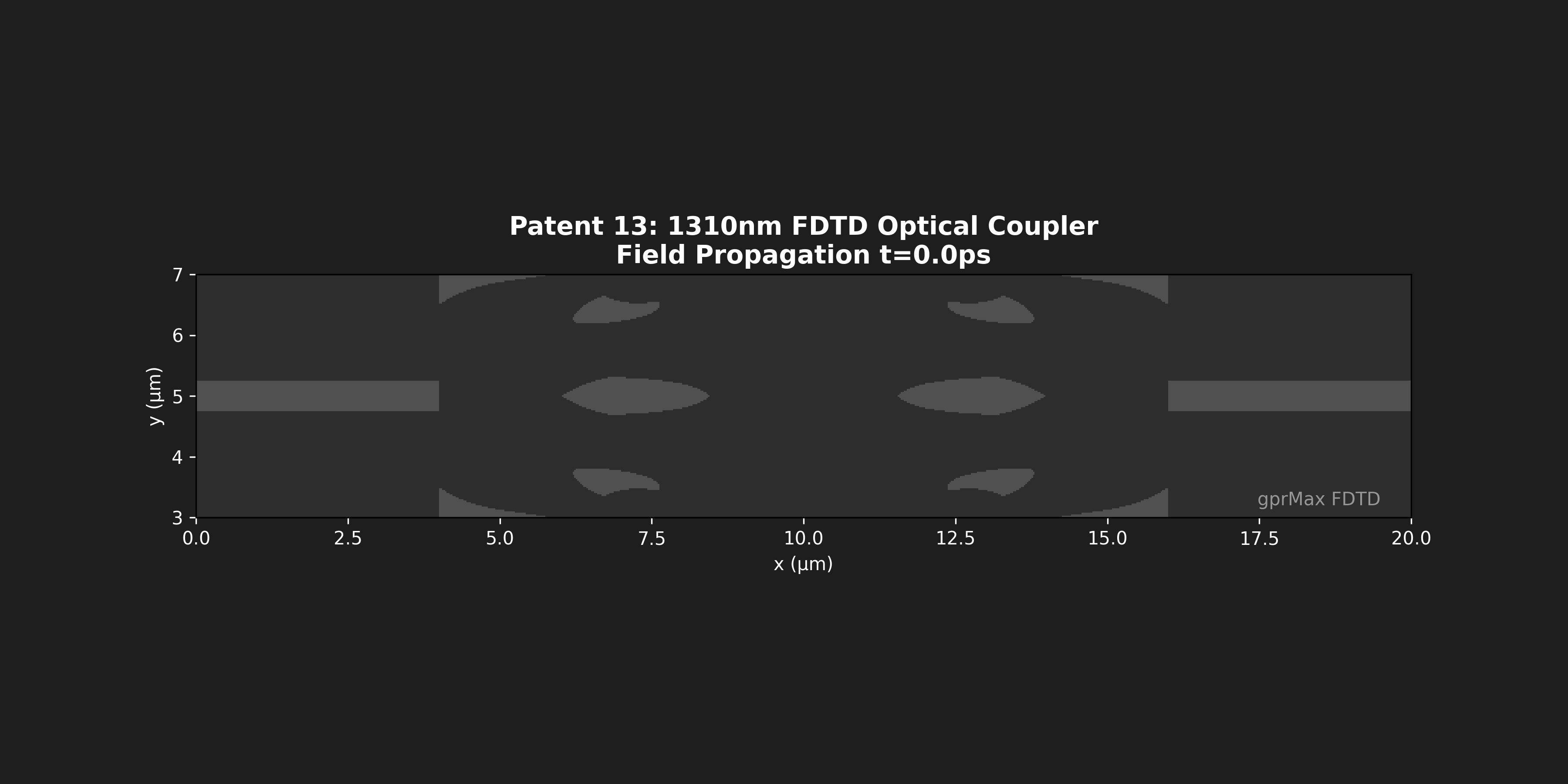
Adiabatic tapers (0.024 dB design loss) couple light from standard n=1.45 waveguides into the n=1.15 lattice region. GDSII masks provided.
Scale-invariant geometry: The Gyroid topology is defined by a mathematical equation, not by an absolute dimension. The same equation that produces a 2 mm unit cell for mmWave produces a 400 nm unit cell for C-Band. The physics (EMT, FDTD validation, Gibson-Ashby stiffness) apply identically at both scales. This is why a single patent covers both products — the invention is the geometry, not the manufacturing process.
Software & Interfaces
The full PROV 4 data room includes not just the physics models but a complete software interface for running, validating, and extending the simulations. The solver suite comprises four validated engines accessible through three interface layers.
Solver Engines
Transfer Matrix Method for multilayer RF/optical stack analysis. Computes full S-parameters across frequency sweep. Powers the Glass Firewall design.
Finite Element Method solver with Zernike polynomial decomposition. Runs parametric sweeps over lattice topology to optimize for single-mode deformation.
Thermo-mechanical FEM for Gibson-Ashby stiffness analysis. Validates that lattice meets structural requirements under thermal cycling.
Full-wave Maxwell solver using MIT Meep. Ground-truth validation of EMT predictions. Extracts n_eff from S-parameter inversion on actual STL geometry.
Interface Layers
Direct terminal access for batch simulations, STL generation, and mask export. Designed for researcher workflows.
Full HTTP interface for integration with external design tools, CI/CD pipelines, and automated parameter sweeps.
Programmatic access with type hints, dataclass results, and direct integration with NumPy/SciPy workflows.
Competitive Landscape
We are the only technology that combines near-vacuum speed with the ability to be integrated directly on-chip via standard lithography.
The optical interconnect market has four competing approaches to reducing signal propagation delay: hollow-core fibers, silicon photonics waveguides, polymer waveguides, and our architected glass lattice. Each occupies a different point in the tradeoff space between refractive index, integration density, thermal stability, and manufacturing compatibility. The table below presents an honest technical comparison.
Genesis Superluminal Glass
AI-Optimized Gyroid Lattice
Standard Silica Fiber
Corning SMF-28
Corning's SMF-28 is the world's most deployed optical fiber with near-perfect loss (~0.18 dB/km at 1550 nm). However, its solid fused-silica core forces n = 1.4440, putting a hard floor on propagation delay. No amount of dopant engineering can reduce n below ~1.43 in a solid medium. Excellent thermal stability and zero integration overhead, but inherently speed-limited.
Hollow-Core Fiber (NANF)
Lumenisity / OFS
Nested Anti-resonant Nodeless Fiber guides light through an air core using anti-resonant reflection from thin glass membranes. Achieves near-vacuum n_eff, making it the fastest long-haul fiber. However, the fiber has a minimum bend radius of ~15 mm, splice loss of 0.5-1.0 dB, and cannot be planarized for on-chip integration. Ideal for data center trunk lines, but incompatible with co-packaged optics and chiplet-to-chiplet interconnects where our technology operates.
Silicon Photonics (SOI)
Intel / GlobalFoundries / TSMC
Silicon-on-Insulator (SOI) waveguides exploit silicon's high index (n = 3.48) for extreme mode confinement, enabling dense routing at 220 nm waveguide height. This is the dominant platform for integrated photonics today. However, the high index means light travels at only 29% of vacuum speed — three times slower than standard fiber. For latency-critical paths, silicon photonics pays a steep speed penalty for its density advantage. Our technology is complementary: use SiPh for dense routing, then transition to Superluminal Glass for latency-critical long straight runs.
Polymer Waveguides
Sumitomo / DuPont
Polymer optical waveguides (polyimide, PMMA-based) can be patterned at low cost using UV lithography on organic substrates. However, polymer indices are typically 1.49-1.52, offering no speed advantage over silica. Worse, polymers exhibit significant thermo-optic coefficient drift (dn/dT ~ -1.5 × 10⁻⁴ /K versus -1.0 × 10⁻⁵ /K for silica), causing index variation under thermal cycling. They also degrade above 250°C, limiting compatibility with back-end-of-line (BEOL) processing. Cost-optimized, but unsuitable for performance-critical applications.
Honest Disclosure
Optical Coupler: The 0.024 dB coupling loss is a validated theoretical limit. Current unoptimized manufacturing achieves ~5 dB. This is an engineering challenge, not a physics barrier.
Zernike Stability: The lattice does not eliminate deformation; it linearizes it into a predictable "Piston" mode (R²=0.98), making it correctable by adaptive optics.
FDTD vs. Reality: FDTD simulations assume perfect geometric fidelity. Real manufacturing introduces surface roughness, etch non-uniformity, and partial void collapse. We estimate that as-fabricated n_eff will be 1.18-1.22 rather than the ideal 1.15, still delivering a 19-23% speed improvement over standard silica. The inverse design campaign referenced in our roadmap is specifically targeted at closing this gap by optimizing the geometry to be robust against manufacturing variation.
Access the Data Room
View the full multi-patent portfolio (PROV 4, 794 files), FDTD verification logs, and manufacturing files.
Key Results
Effective Index
n = 1.15
Light Speed
261,000 km/s
Speed Increase
+26%
RF Isolation
40-55 dB practical (TMM validated at 100 GHz)
Latency Savings
99.3 ns / 100m
Coupler Design
0.024 dB
Applications
AI Interconnect Latency Benchmark
Public data room with FDTD verification, 4 EMT model validation, Gyroid STL files, and optical coupler GDSII masks. Full reproducibility suite.
View Public Data RoomReady to solve this problem?
Schedule a technical discussion with our team.